Meizhou Ruiputuo Technology Co.,Ltd
 In PCB wiring, the planning and layout of ground wires and power wires are very important, which can affect the stability, anti-interference ability and signal quality of the circuit. Here are some common planning and layout suggestions:
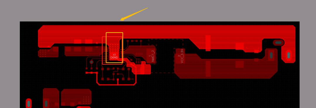
Separate ground planes: Divide the ground wire into two areas: analog ground and digital ground, and use two independent ground planes for routing. This can prevent mutual interference between analog signals and digital signals. The distance between analog ground and digital ground should be no less than 1mm. If it cannot be drawn so wide due to structural limitations, it can be appropriately reduced.
Use copper laying and shielding: Lay copper foil on the ground area of the circuit board to form a ground plane, which effectively reduces the resistance and inductance of the ground wire and improves the circuit's working stability and anti-interference ability. In addition, use a shielding cover It can also isolate the ground wire and power wire to a certain extent to reduce interference and electromagnetic radiation.
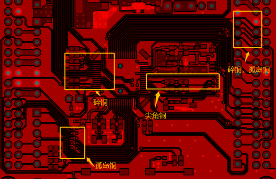
But it should be noted that when laying the entire copper sheet, we need to dig out the "useless" copper sheet, such as some broken copper, sharp-angle copper sheet, island copper, etc. These copper sheets not only cannot provide shielding The effect will also affect the signal quality.
Width and arrangement of power cords: Power cords should be wide enough to provide adequate current transfer capabilities and should be kept as direct and short-distance as possible to reduce resistance and inductance.
Ground wire wiring: The ground wire plays the role of loop closure in PCB wiring and should form a loop as complete as possible. Avoid the ground wire being too long or too thin and reduce the resistance and inductance of the ground wire.
From other circuit modules: The power supply should be separated from other signal modules as much as possible. The power supply needs to be clearly distinguished from other circuit modules. The power plane and high-speed, low-voltage and high-voltage parts must be distinguished to a certain extent.
Splitting the power supply: Especially for multi-voltage and noise-sensitive circuits, power splitting technology can be used in the PCB to separate power lines of different voltages to reduce mutual influence. Usually we will also do certain things for different power supply voltages. For degree processing, generally when the potential difference is greater than 12v, the separation distance is not less than 50mil. On the contrary, a spacing of 20-25mil can be selected.
Good grounding: In PCB, the selection and layout of grounding points is very important. You should choose a low-impedance, low-noise ground point, and try to place the ground point in the center of the circuit to facilitate wiring.