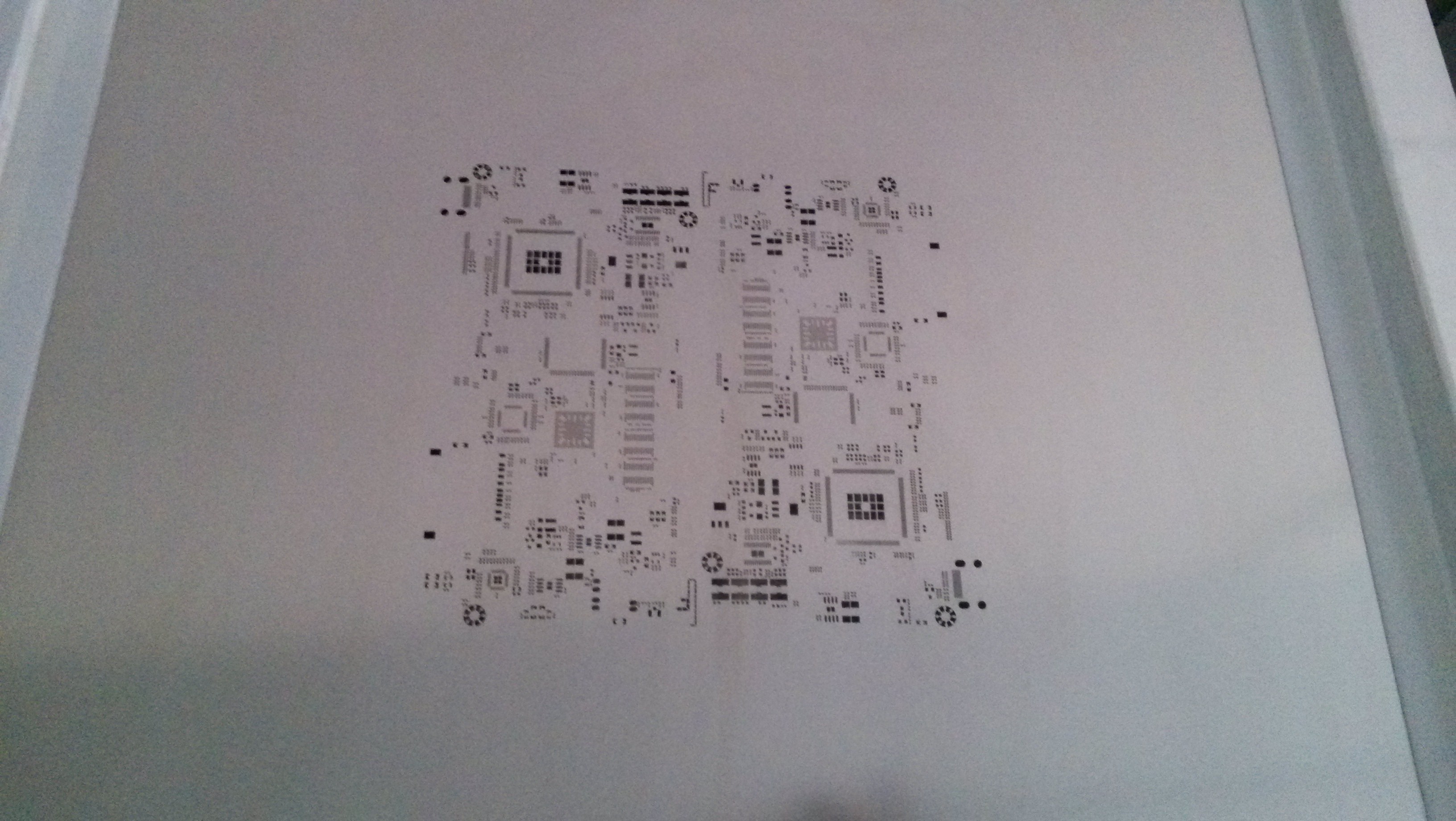
Analysis of three kinds of PCB steel mesh technology
1, solder paste steel mesh: as the name suggests is used to brush the solder paste. Cut holes corresponding to pcb pad on a steel sheet. The solder paste is then pad printed onto the PCB board through the steel mesh. To print the paste, apply the paste to the top of the mesh and the circuit board to the bottom of the mesh, then use a scraper to scrape the paste over the mesh (the paste will run through the mesh and over the circuit board when squeezed). Attach the patch components, unified reflow welding, plug-in components manual welding.
2, red rubber steel mesh: opening is according to the size and type of parts to open in the middle of the two welding disc components. The use of dispensing (dispensing is the use of compression air, the red glue through the special dispensing head point to the substrate) the red glue through the steel dot to the PCB board. Then put on the components, such as components and PCB stick stable, plug in the plug-in components unified wave soldering.
3, double process steel mesh: when a PCB board needs to brush solder paste, and need to brush red glue, then you need to use double process steel mesh. The double process steel mesh consists of two steel mesh, a common laser steel mesh, a stepped steel mesh. How to determine the use of solder paste ladder steel net or red glue ladder steel net? First know whether to brush the solder paste or brush the red glue first. If it is the first brush solder paste, then solder paste steel net to make ordinary laser steel net, red rubber steel net to make ladder steel net. If it is first brushed with red glue, then the red glue steel net is made into ordinary laser steel net, and the solder paste steel net is made into ladder steel net.

 Meizhou Ruiputuo Technology Co.,Ltd