 Meizhou Ruiputuo Technology Co.,Ltd
The specific content of PCB design
It is recommended to use 4 or 6 layers for PCB design
Note: The second layer and the third layer can be interchanged, determined according to the layout level of the main components. Its immediate adjacent layer is the ground.
Note: The second layer and the fifth layer can be interchanged, determined according to the layout level of the main components. Its immediate adjacent layer is the ground.
formation
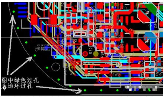
Create a ground ring around the PCB with vias. The smallest via used is 0.254mm. 0.3mm vias are recommended. The pitch of each via is between 1.27mm and 2.5mm. Use vias on every side of every layer as much as possible. as shown in the picture
power layer
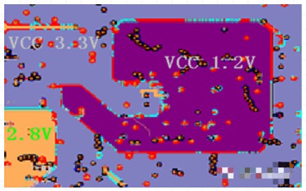
Divide the power supply layer to distribute each independent power supply. The independent power supplies are as follows:
Provided to the DSP core and analog power supply.
Provided for digital I/O ports and peripherals.
The purity of 2.8V and VCC (provided to the camera power supply) is the guarantee of good image quality
。
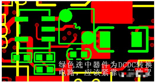
The DC/DC converter places a 10uH power inductor on the DC/DC output SW pin as close as possible to the SW pin. And the wiring as much as possible is at least 0.6mm. A good suggestion is to put the DC/DC chip and the power inductor on the same side of the PCB as much as possible. If they are not on the same side of the PCB. It is necessary to use multiple vias to connect the power inductor to the SW pin. The power filter capacitor at the power input end of the DC/DC converter is preferably a tantalum capacitor.
When the DC/DC chip is used, the value of the tantalum capacitor is recommended to be 4.7uF or 10uF. Or use a capacitor with a low ESR value. And the output terminal of the power inductor is preferably connected with 0.1uF and 10uF capacitors. These capacitors should be placed as close as possible and at most 4mm away from the output of the DC/DC IC. The placed 0.1uF decoupling capacitor is best placed in front of the 10uF capacitor.
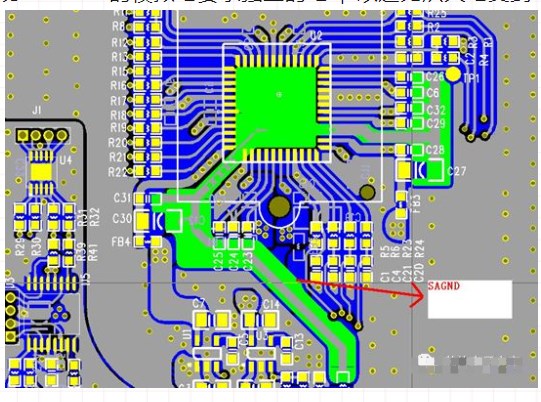
It is better to separate the analog ground and the digital ground and connect them through an inductor or a 0 ohm resistor. If the board is too small to separate the analog and digital grounds, they can be connected directly, but the ground loop of the digital signal should not affect the analog part.
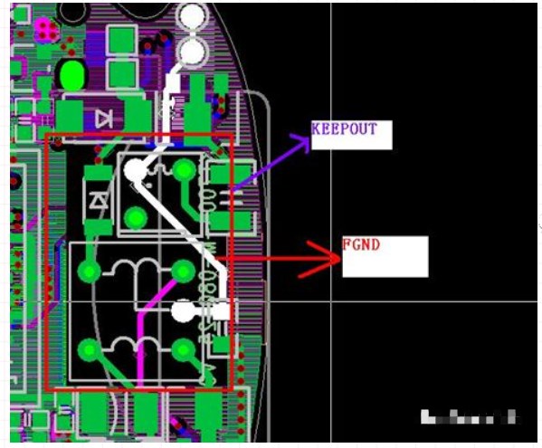
In order to help improve the quality of the analog part, they each go through their own ground loops. This is to prevent the analog part from coupling the digital signal from the digital ground. Especially for audio ground and SENSOR ground. The ground of the flash: please do not lay copper on FGND, and it is better to keep this network at least 3mm away from other components and networks
。
All Audio traces should be as wide as possible. All components for audio output should be placed as close as possible to the headphone socket. It is recommended to put these audio-related components and wiring together, and try to be in the same part of the PCB as the system audio output. Try to avoid coupling noise from other signals. The width of audio output traces is not less than 0.254mm.
The audio signal line of the earphone layout should be far away from the data lines and control lines of NAND Flash, as well as high-frequency signals, and away from the crystal oscillator circuit. If the audio signal lines are routed too close to these signal lines, the quality of the audio will be affected.
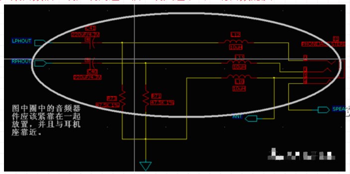
(Remarks: The audio components in the above picture should be put together and as close as possible to the audio input and output sockets. The wiring should be as wide as possible. Avoid vias, avoid crossing digital and analog grounds. The ground ring of the Audio part Multiple returns and loops are not allowed.)
AUDC_VREFADC, AUDC_VREFDAC, AUDC_VCM signal filter tantalum capacitor 10uF and ceramic capacitor 0.1uF should be as close as possible to the main control IC. Its traces need to be kept away from high-frequency digital signals. Such as SDRAM, NAND FLASH data lines, address lines and control lines.
The audio input signal line from the microphone should be far away from the data line and control line of NAND Flash, as well as high-frequency signals, and away from the crystal oscillator circuit. If the MIC input signal line is too close to these signal lines, it will affect the quality of audio input. The MICBIAS analog lines should be kept away from DC/DC power inductors, digital signal lines, control lines and crystal oscillator circuits. Place the filter components as close as possible to the microphone. The MIC input signal needs to be separated from the MICBIAS power signal. Avoid mutual interference. It is best to do packet processing on the MIC input signal. The microphone ground should be separate from the digital ground. Avoid coupled digital noise.
Line in considerations
The signal line of the input headphone socket of Line in should place a separation resistor at its input end. Protect the chip from being damaged by the impact of the input signal. Components related to Line in should also be placed together as much as possible. The ground is also separate from the digital ground.
Sensor considerations
The power supply of Sensor requires very stable and pure 2.8V and 1.8V power supply. Therefore, it is recommended that LDO and large-capacity bile capacitors be used in this power supply section. The analog ground of the Sensor requires an independent ground ring. to avoid disturbing noise from the ground
.
USB Considerations
The differential signal lines of the USB are kept in parallel to achieve a differential impedance of 90 ohm. Due to PCB and routing factors, such parallel routing requirements are difficult to achieve. To avoid such deviations, reduce as much as possible. It is recommended that the width of the trace is not less than 0.254mm, and the spacing of the differential signal lines is not less than 0.254mm. This is as close as possible to the differential impedance of 90 ohm.
High-speed USB
In order to obtain ideal signal quality, it is recommended that the distance between the differential signal lines of high-speed USB and other signal lines should be more than 0.5mm. This helps avoid interaction interference. Another option to achieve a differential impedance of 90 ohm. You can add 6pF to ground on the differential signal line pair of USB. Because some designs require these, but when some PCB designs do not reach the differential impedance of 90 ohm they need these. PCB layout, these pads need to be kept when needed.
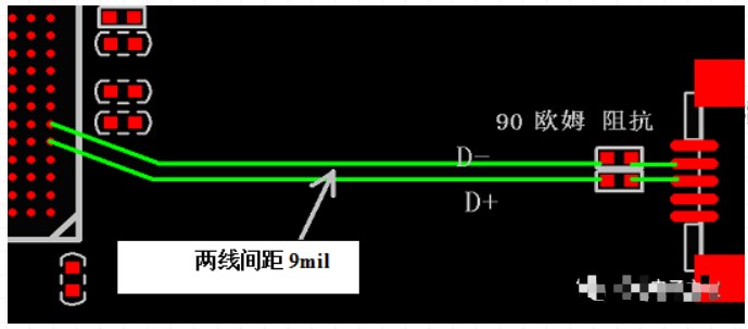
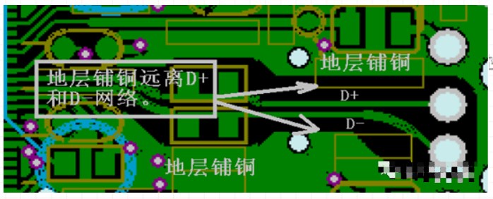
The line width and line spacing of D+ and D- are 9mil. Copper should not be laid next to these two signal lines, and the ground should be bare. As shown below:
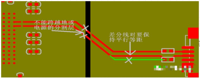
Some poor USB traces
Some very common bad USB traces are USB traces that use too many vias. Separation layer spanning the power and ground lines. The ground lines on both sides of the USB signal pair are asymmetrical. Non-parallel signal pairs and too many vias will cause impedance discontinuity which will lead to poor signal quality
。
SDRAM part routing considerations
1. SDRAM clock signal The frequency of the clock signal is relatively high. In order to avoid transmission line effects, according to the principle that the wiring length should be within 1000mil when the operating frequency reaches or exceeds 75MHz and to avoid crosstalk with adjacent signals, the wiring length should not exceed 1100mil and the line width should be 10mil. , 20mil distance from other external signals. The best land. 2. Address, chip select and other control signals: line width 5mil, distance between control signals of the same type is 10mil, distance from other external signals is 20mil, as few vias as possible, preferably within 2. Do equal-length trace processing with the clock signal. 3. SDRAM data line: the line width is 5mil, the distance between the same type of data signal is 5mil, and the distance between other external signals is 10mil, and the wiring should be on the same layer as much as possible. The length of the data line and the clock line should be equal in length.
ESD considerations
The PCB design that requires good ESD is recommended to use a 6-layer PCB design with independent power and ground layers. All component pads should be connected to the earth ground pad. Ferrite beads should also be connected between each signal line and the peripheral. The varistor should also be added to each signal line of the USB, the audio signal line and the signal line of the button to the ground. Buttons and switches should use insulator components as much as possible. The USB socket should be covered by non-conductor gel. If metal or conductors are used, it should be designed so that the electrostatic current is evenly distributed around the PCB board. The air gap between the keys and switches and the PCB should be as small as possible. Avoid headphone jacks with metal outer rings.
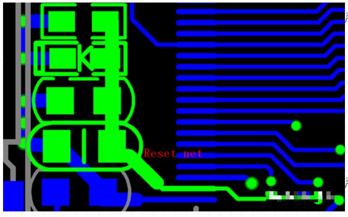
About the reset circuit part. Connect a 68pF ceramic filter capacitor in series between the reset pin and the ground. All components of the reset circuit should be as close as possible to the reset pin of the chip. The reset trace should be as short as possible. If the trace is long, go to the middle layer. As shown below
When discharging static electricity to the PCB, it is for more ground distribution of charges. It is very helpful to place as many ground VIAs as possible around the PCB.
The 0.01uF filter capacitor is connected across the NC pin of the LDO of USB_VDD33 and VDD33 to ground. Filter out the instantaneous impact of static electricity on the power supply.
The chip code power supply network is the antistatic stability of the chip core power supply. Need to add 68pF and 0.01uF ceramic capacitors to ground. And as close as possible to the pins of the chip.
Increase the area of the land as much as possible. And make the formation as complete as possible. The power wiring of the whole machine should be as thick and short as possible. Power and ground loops should be as small as possible. Only in this way can the static electricity be released quickly.
The shell of the crystal oscillator should be grounded. The shell of the USB is connected to DGND through a 0.1uF capacitor. DGND near the USB should be drilled as many holes as possible.
EMI considerations
Place 0.1uF filter capacitors on the corresponding power supply pins. Place the 10uH DC/DC power inductor as close as possible to the SW pin of the DC/DC converter, and use a power inductor wrapped with a magnetic ring. This helps to suppress the noise of higher harmonics of DC/DC conversion. Place the filter capacitors of 0.1uF and 10uF as close as possible to the output end of the power inductor. Digital signal lines should be routed on the inner layer as much as possible. The routing of the clock signal line should be as short as possible. Some EMI devices can be added to important signal lines when necessary.