 Meizhou Ruiputuo Technology Co.,Ltd
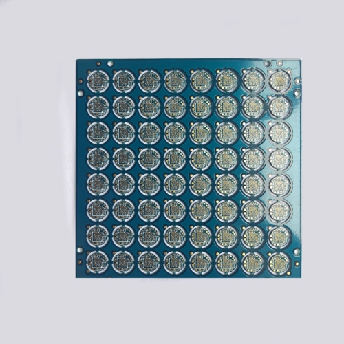
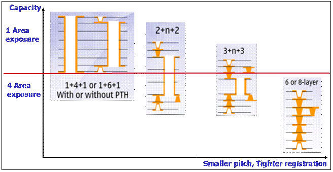
1. Simple one-time laminated printed board (one-time laminated 6-layer board, laminated structure is (1+4+1)) as shown below
HDI circuit board stack structure diagram
This type of HDI board is the simplest, that is, there is no buried hole in the inner multilayer board, and it can be completed in one press. Although it is a laminated board, its manufacture is very similar to the conventional multilayer board. The difference is that multiple processes such as laser drilling blind holes are required. Since there is no buried hole in this laminated structure, in the production, a core board can be made on the 2nd and 3rd layers, and another core board can be made from the 4th and 5th layers, and the outer layer is added with a dielectric layer and copper. The foil is laminated with a dielectric layer in the middle, which is very simple, and the cost is lower than that of conventional primary laminates.
2. Conventional one-time laminated HDI printed board (one-time laminated HDI 6-layer board, stacked structure is (1+4+1)) as shown below
The structure of this type of board is (1+N+1), (N≥2, N even number), this structure is the mainstream design of the primary laminated board in the industry at present, and the inner multi-layer board has buried holes, which requires secondary Pressing is complete. This type of primary laminate has buried holes in addition to blind holes. If the designer can convert this type of HDI into the simple primary laminate of the first type above, it will be beneficial to both the supply and demand sides. is beneficial. Many of our customers have been suggested by us, and it is preferable to change the laminated structure of the second type of conventional primary laminate to a simple primary laminate similar to the first type.
3. Conventional secondary laminated HDI printed board (secondary laminated HDI 8-layer board, stacked structure is (1+1+4+1+1)) as shown below
The structure of this type of board is (1+1+N+1+1), (N≥2, N even number), this structure is the mainstream design of the second layer build-up in the industry, and the inner multi-layer board has buried holes, It takes three presses to complete. The main reason is that there is no stacked hole design, and the production difficulty is normal. If the buried hole optimization of the (3-6) layer can be changed to the buried hole of the (2-7) layer as mentioned above, one pressing can be reduced and the optimized process to reduce costs. This type is like the example below.
4. Another conventional secondary laminated HDI printed board (secondary laminated HDI 8-layer board, stacked structure is (1+1+4+1+1)) as shown below

The structure of this type of plate (1+1+N+1+1), (N≥2, N even number), although it is the structure of the secondary laminate, but because the position of the buried hole is not in (3-6) Between the layers, but between (2-7) layers, this design can also reduce the pressing once, so that the HDI board that is laminated twice needs 3 times of pressing process, which is optimized to 2 times of pressing process . And this kind of board has another difficulty in making, there are (1-3) layers of blind holes, which are split into (1-2) layers and (2-3) layers of blind holes to make, it is necessary to make (2) -3) The inner blind hole of the layer is made by hole filling, that is, the inner blind hole of the secondary layer is made by the hole filling process. Usually, the cost of HDI with the hole filling process is lower than that without the hole filling process. Therefore, in the design process of conventional secondary laminates, it is recommended not to use stacked hole design as much as possible, and try to convert (1-3) blind holes into staggered (1-2) blind holes and (2-3) Buried (blind) holes. Some experienced designers can adopt this design or optimization to reduce the manufacturing cost of their products.
5. For the HDI of the secondary laminate of the blind hole stacked hole design, the blind hole is stacked above the buried hole (2-7) layer. (Secondary laminated HDI 8-layer board, the stacked structure is (1+1+4+1+1)) as shown below
The structure of this type of panel is (1+1+N+1+1), (N≥2, N even number), this structure is currently part of the industry's secondary laminated panels have such a design, the inner multi-layer The board has buried holes, which need to be pressed twice to complete. There are mainly stacked hole design and cross-layer blind hole design. The main feature of this design is that blind holes need to be stacked above (2-7) buried holes, which increases the difficulty of production. The buried holes are designed on (2-7) layers, which can One lamination is reduced, the process is optimized and the cost is reduced.
6. Secondary laminated HDI with cross-layer blind hole design (secondary laminated HDI 8-layer board, stacked structure is (1+1+4+1+1))
The structure of this type of panel is (1+1+N+1+1), (N≥2, N even number), this structure is a secondary laminated panel that is currently difficult to manufacture in the industry, such Design, the inner multi-layer board has buried holes in the (3-6) layer, which needs three times of lamination to complete. The main reason is that there is a cross-layer blind hole design, which is difficult to manufacture. It is difficult for HDI PCB manufacturers without certain technical capabilities to make such secondary laminate parts. If this kind of cross-layer blind hole (1-3) layers, optimize the split For (1-2) and (2-3) blind holes, this method of splitting blind holes is stacked hole splitting method, but the splitting method of staggered blind holes will greatly reduce the production cost and optimize the Production Process.
7. Optimization of HDI boards with other laminated structures
three-time laminated printed boards or PCB boards with more than three laminated layers can also be optimized according to the design concept provided above. For a complete three-layered HDI board, the entire production process requires 4 times of lamination , if the design ideas similar to the above-mentioned one-time laminated board or two-time laminated board can be considered, the production process of one-time lamination can be completely reduced, thereby improving the yield of the board. Among our many customers, there are many such examples. The laminated structure designed at the beginning requires 4 times of lamination. After the optimization of the laminated structure design, the production of PCB only needs 3 times of lamination. It meets the functions required by the three-time laminated board, thereby greatly improving the production efficiency and reducing the production cost.


