 Meizhou Ruiputuo Technology Co.,Ltd
 Modern PCB layout software allows engineers, designers and enthusiasts to quickly and easily design PCB. The software provides creative freedom, but sometimes this is not a good thing. PCB designers may make a hasty design error. These errors will not affect the function of the product, but it may affect assembly, debugging and yield, because these hasty errors cause confusion. This article introduces some basic hasty PCB design style errors and how to avoid these errors.
Modern PCB layout software allows engineers, designers and enthusiasts to quickly and easily design PCB. The software provides creative freedom, but sometimes this is not a good thing. PCB designers may make a hasty design error. These errors will not affect the function of the product, but it may affect assembly, debugging and yield, because these hasty errors cause confusion. This article introduces some basic hasty PCB design style errors and how to avoid these errors.
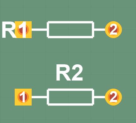
Reference mark under the pad pad
The reference mark on the copper will appear in the PCB layout software, but it will not appear on the physical PCB. If your reference indicator is placed on the pad in the layout, they will be lost when you get the PCB, and it will be difficult to place the component. In the figure below, the reference mark of the R1 will not be completely printed on the PCB. "1" will be cut off. The reference label of R2 is placed correctly.
It may destroy the PCB layout style error you designed
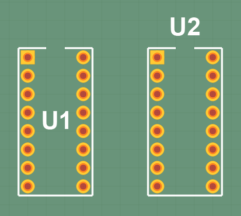
Reference mark under packaging
If you place reference tags under the component, you or your contract manufacturer may be able to place the component, but if you need to remove or replace the component for maintenance or debugging, it is difficult to find the component on PCB. In the figure below, after U1 is placed on the PCB, the reference mark of U1 will be hidden. After the U2 is placed, the reference mark of the U2 will be clearly visible.
It may destroy the PCB layout style error you designed
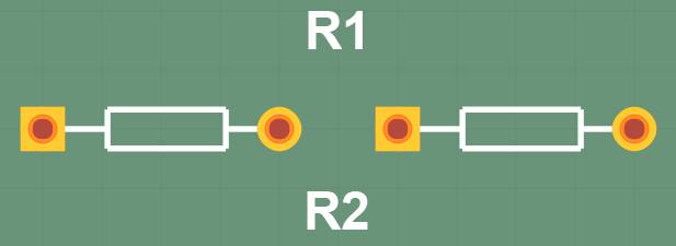
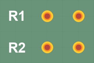
The reference mark that is not clearly assigned to the component
Place the reference mark as close to its components as possible. Place the reference indicator in some way to know which components they belong to. If you don't do this, it will be difficult to place the correct component in the correct position. This is important for assembly and debugging. In the figure below, it is not clear which resistance is R1 and which is R2.
It may destroy the PCB layout style error you designed
Use enough reference indicator fonts that are large enough to read. The author has successfully used the fonts of at least 0.060 "height and 0.050". This prompt does not have pictures, because any size reference indicator looks good on large high -resolution displays, especially when you are magnified.
A component with a vague reference indicator approaching each other
The components are placed adjacent to each other. The reference label does not clearly indicate which components can cause many problems on which pads can be caused, including the wrong components are placed on the wrong pad Essence The author has seen this error layout, as shown in the figure below. Some PCBs made with this layout and the horizontal -placed resistor are assembled correctly. The resistors of other PCB are not correctly placed. The dislocation of this parts makes PCB unable to work. Using contours around the component is a method to avoid this problem.
It may destroy the PCB layout style error you designed
The reference mark on the PCB should be directed to one or more directions. Random orientation reference indicators make assembly and debug more difficult, because components are more difficult to find. The component on the left has an appropriate reference indicator. The component on the right has a reference indicator in different directions, which is bad.
It may destroy the PCB layout style error you designed
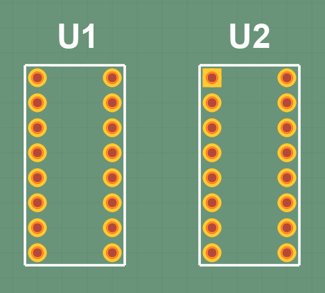
Not marked on the integrated circuit to quote the foot 1
The integrated circuit should have a clear indicator next to the pin 1, such as point or star shape to ensure that the IC installation is correct. Improper installation ICs may be damaged or destroyed. When the IC is on the PCB, if the pin 1 indicator is not buried below the IC, debugging will be easier. In the figure below, U1 will be difficult to place correctly. Please note that the pin number you see in the picture will not appear on the PCB. U2 will be placed correctly because pin 1 has been clearly marked (square pins).
It may destroy the PCB layout style error you designed
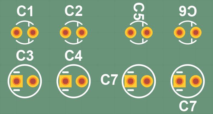
The polarity of non -marked polarization elements
Some ends such as LED and electrolytic capacitors are polarized. Error installation of polarization components can cause circuit failure or component damage. LED will only shine when the correct installation is installed. If the installation is reversed, the LED will not be turned on, and may even be broken by voltage. If reverse bias, electrolytic capacitors will explode. Use footprints with polarity. The polar marks should not be buried below the component. In the figure below, the package of C1 is not good because polar marks will be covered by components. The package of C2 is very good, because when the capacitor is located on the PCB, you can see the polar mark.
It may destroy the PCB layout style error you designed
Placement of components too close will cause problems such as welding bridges. If the component distance is too close, it may be difficult to use the oscilloscope or the multimeter for detection, because the probe may be connected to multiple components together. Placement of components too close will also make the replacement component difficult. This is seen on PCB, because the component spacing may look good on a large display.
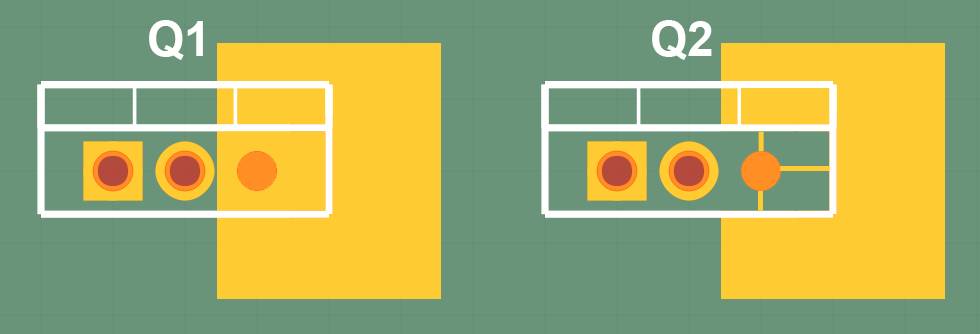
Use the cooling device on the component pin to make welding easier. You may not want to use thermal release to reduce the resistance and thermal resistance, but not using the heat release will make the welding very difficult, especially when the component pad is connected to a large walk or copper filling. If the proper heat dissipation device is not used, large routing and copper filling will be used as a radiator, which will make it difficult for heating pads. In the figure below, there is no heat sink on the source of Q1. The MOSFET may be difficult to weld and welded. The source of Q2 is released by heat. The MOSFET is easy to weld and welded. PCB designers can change the heat dissipation to control the connected resistance and thermal resistance. For example,
It may destroy the PCB layout style error you designed
Understand the limitations of PCB manufacturers, contract manufacturers and you
With a set of good design rules, your PCB manufacturer can meet these rules.
Understand whether you or your CM can handle difficult packages like the ball array. If you welded yourself, the packaging on the side of the IC package is easy to weld, especially when the spacing is not too small (less than 0.100 ").
in conclusion
This article covers some PCB layout styles that may lead to assembly and debugging issues. Keep in mind the reference mark carefully, use good packaging with polarity and pins 1 mark, use the cooling device, and consider manufacturing restrictions during design. Following these good design practices will make the assembly easier, improve the yield and make debugging easier. These benefits can save time and money, so that you can worry about it.